
Theremin PCB - see you on the component side
When we left off last time, I had just put the finishing touches on the copper-trace side of my theremin circuit board. This included sanding copper off of the other side of the PCB; I removed the copper - but despite my best buffing efforts I could not return the board to its smooth state. Read on to find out how this turns out.
Materials needed for creation of the flip-side of theremin PCB:
- copper-trace side of board from previous steps completed
- image of component side of PCB printed recently on glossy paper from laser printer (check Chris's RS Theremin site for more info)
- iron
- paper
I ironed alot, because I noticed that some areas of the paper were not showing any toner. The paper came right off after I stopped, and it looked really bad. So I tried again with a new printout on the same board, and this is the best I could get.
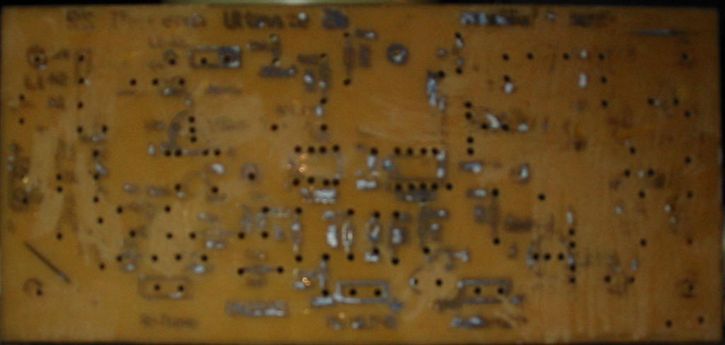 If you look close, you will notice that all the areas that the silkscreen image did not transfer are the scuffed areas where I sanded the remaining copper off.
I decided that putting all the components on this board might end up being a waste of components because in some areas on the other side the copper traces were far less than perfect. I will make a new board as soon as possible, stay tuned for more theremin updates shortly!
I think I just might have found the perfect enclosure to put my first theremin in ...
posted by DanO @ 1:15 AM
![]()
1 Comments:
I was looking for this info for many days related to theremin pcb.. Great blog fr me to get info material from it..
Post a Comment
<< Home